SFB Extra Seminar
Tunable as-grown graphene contacts to semiconducting transition metal dichalcogenides
| Datum: | 28.01.2019, 11:00 - 13:00 Uhr |
| Kategorie: | Seminar |
| Ort: | Hubland Süd, Geb. P1 (Physik), SE 6 |
| Veranstalter: | SFB 1170 ToCoTronics |
| Vortragende: | Shruti Subramanian - Penn State University |
Heterogenous combinations of two-dimensional (2D) layered materials provides us with an ability to tune several electronic and optical properties tailored for specific applications. Transition metal dichalcogenides (TMDs) are attractive 2D materials in the “beyond graphene” realm of materials. To utilize their unique electronic properties, it is important to develop low resistance contacts to these materials. Graphene is a promising candidate and has been shown to produce low-resistance contacts to a few TMDs. But this has been done by manual stacking via exfoliation or polymer-assisted transfer, which is not a scalable method. One avenue that is still in its infancy, yet could provide significant potential for scalability and be enroute “all-2D” electronics is the realization of as-grown graphene contacts to 2D materials beyond graphene. Here, I discuss electronic properties resulting from the interface of the as-grown lateral heterostructures between epitaxial graphene and TMDs.
Using powder vaporization to grow the TMDs on patterned epitaxial graphene, directly yields 2D lateral heterostructure between graphene and TMDs like MoS2, without the need for transfer of any 2D layers. Investigation of this synthetic lateral heterostructure via several advanced characterization techniques leads to an understanding of the structure of this interface. Cross-sectional transmission electron micrography shows that the interface between graphene and MoS2 is in fact, a pristine overlap of the MoS2 onto the graphene for a few hundred nanometers. This unique combination allows for improved electronic coupling and reduced contact resistance to these TMDs using graphene as the contacting material instead of conventional metals like Ti/Au. The flexibility of being able to tune the doping of the epitaxial graphene allows us to explore the option of type-matching the graphene contact to the doping of the TMD, thus reducing the barrier for electrons and making contacts much superior to conventional metals.
This talk will also expand on the extensive efforts being made in the field of 2D materials at Penn State
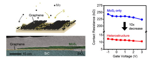
Figure 1: High left - Schematic showing the growth of MoS2 on patterned graphene. Lower left – Cross sectional HRTEM image showing the overlap of the graphene and MoS2 at the heterostructure interface. Right – Contact resistance reduction via introduction of as-grown graphene contacts to MoS2