Nanophysics at surfaces
Overview of research: Electronic Interactions in Atomic Nanostructures and in Low Dimensions
The research activities of our group are concerned with the physics of low-dimensional systems, where the electron states resulting from dimensional confinement lead to unusual conduction properties and to phase transitions as a function of temperature. These can include charge density waves (CDW), spin density waves (SDW), as well as Mott-Hubbard (MH) metal-insulator transitions. Moreover, in one-dimensional systems the physics can be drastically different from what is known in three-dimensional matter, and even the Fermi liquid picture may no longer be valid. It is fascinating to see how phase transitions between the conducting and insulating state for example are in fact driven by an electronic mechanism. In the case of a CDW, an electronic nesting condition governs the instability, while for an MH transition the local Coulomb interaction comes into play.
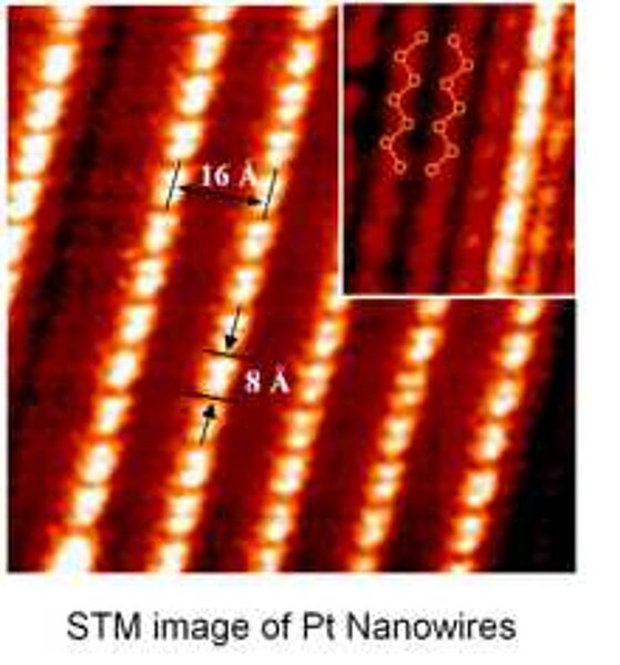
Systems: Realizations of such low-dimensional systems are intensely sought-after, and can be obtained in different ways. One class of quasi-1D systems are compound crystals with rather directional bonds, which exhibit electron states that are highly confined to one dimension. Another realization are systems prepared on surfaces of solid state substrates. These include self-organized growth of metal adsorbates on semiconductor surfaces. This method allows to tune the dimensionality between 2D and 1D behavior. Moreover, even the bare surface by itself is a realization of a 2D system, leading to the formation of surface states. Such well-defined states lend themselves to the study of many-body interactions and their particular energy scale. A key advantage of such surface-prepared systems is the relative ease with which they can be accessed by spectroscopic methods. They offer the unique possibility to modify them by e.g. exchange of the adatom species, or by modification of their charge content through doping. This allows an exceptional degree of control over the electronic properties.
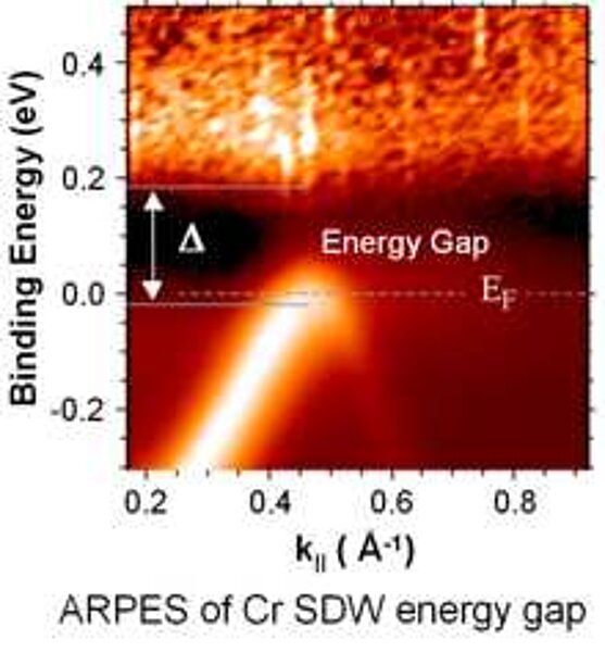
Techniques: The experimental techniques are based on ultra-high vacuum surface preparation of semi-conductor substrates and metals, wet-chemical etching in a flow box environment and electron-beam epitaxy of adatoms. Angle-resolved photoelectron spectroscopy (ARPES) with imaging analyzers is used to study the electronic states with high resolution. We specialize in spectroscopy of states at the Fermi level, in order to resolve energy gaps of charge density waves and 2D Mott systems as fingerprint of phase transitions. Part of the studies make use of synchrotron radiation with high brilliance and tunable photon energies. Scanning tunneling microscopy (STM) is used for structural determinations and especially to study the formation of CDW periodicities. The in situ combination with ARPES allows access to both real space and reciprocal space and thus the electron-lattice interplay.