Molecular Beam Epitaxy

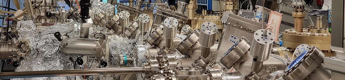
We are operating eight chambers for molecular beam epitaxy (MBE) of various group II-VI, III-V, IV-IV, IV-VI, V-VI semiconductor, half-Heusler, and superconducting crystalline layer structures. Six of the MBE chambers, a sputtering, a metallization, and a surface analysis chamber are connected to a cluster by an ultra-high vacuum (UHV) transfer system. This setup enables the very flexible fabrication of high-quality heteroepitaxial layer structures, in-situ ohmic contacts, superconducting contacts, dielectric layers, and surface protection layers. The composition and thickness of the epitaxial layers are mainly controlled by the offered molecular beams at adequate growth conditions with an accuracy of about 1% and 1 atomic layer, respectively. The used substrates with various materials, crystal orientations, strain-relaxed buffer layers, and the layer properties define the resulting electronic band-structure of the epitaxial multiple layer structures. Our research activities and MBE developments were historically aimed in studying II-VI and III-V semiconductor devices in electronic and spintronic magneto-transport, as well as optical spectroscopy.
This research has enabled the first observation of the quantum spin Hall effect by quantum transport in spin-momentum locked electron edge channels of a thin HgTe/CdTe layer structure in 2007. HgTe is a representative of the new class of matter of a topological insulator (TI). They are characterized by an inverted electronic band-structure, strong spin-orbit coupling, resulting topological surface states, insulating properties of the bulk, and dissipation-less conductance of edge states. Consequently, TIs require high-purity layers with high-quality interfaces and surfaces. The topological properties of pseudomorphic layer structures can be designed by composition, quantum confinement, heteroepitaxial strain, electronic doping, and alloying by magnetic elements. The layer properties combined with the lithographic processing of macroscopic or advanced nano-scale devices enable quantum transport studies of their topological electronic phases and novel physics.
Our studies of various topological materials and their properties have developed rapidly since 2007:
- The outstanding HgTe/CdTe material system represents TIs in 2 and 3 dimensions, Weyl and Dirac semi-metals, dilute magnetic TIs, induced superconductors, or just usual semiconductors depending on layer and device design.
- Van-der-Waals-bound (Bi,Sb)2(Te,Se)3 layers alloyed by V or Cr are ferromagnetic 2D and 3D TIs and reveal quantum anomalous Hall and axion insulator properties.
- (Pb,Sn)(Te,Se) layers represent topological crystalline insulators with multiple surface states protected by crystal symmetry.
- The half-Heusler materials YPtBi and FeSe are topological and unconventional superconductors.
- Alloying of narrow bandgap (Hg,Zn,Cd)Te and wide bandgap (Zn,Cd,Be)Se by Mn enables semi-magnetic TI and spintronic devices.
- Special MBE growth modes like the Stranski-Krastanov and vapor-liquid-solid mode allow the epitaxial fabrication of self-assembled quantum dot and quantum wire structures.


MBE is a very advanced method for the deposition of thin heteroepitaxial layers on a single-crystal substrate by thermal evaporation of elemental materials at UHV conditions. In principle, this is a physical and controlled growth mode, but high-quality layers require optimized growth conditions. The TI materials HgTe and VI2VI3, the stochiometric superconductors YPtBi and FeSe, and some alloyed layers require fluxes and a substrate temperature to be accurate within a percent.
The properties and quality of the MBE-grown layers and heterostructures are continuously developed and improved. The methods applied for structural characterization are:
- In-situ reflection high-energy electron diffraction (RHEED)
- High-resolution x-ray diffraction (HR-XRD) and x-ray reflection (XRR)
- Atomic force microscopy (AFM)
- Scanning electron microscopy (SEM)
- Energy-dispersive x-ray spectroscopy (EDX)
- Scanning tunneling microscopy (STM)
- (Scanning) transmission electron microscopy (S-TEM).
The electronic, topological and magnetic properties are characterized in close cooperations with the groups in EP 3, ITI, the University Würzburg and external institutions by:
- Magnetotransport
- (Angle-resolved) photoelectron spectroscopy (AR-PES)
- Resonant x-ray spectroscopy
- Optical spectroscopy (THz – UV)
- Scanning quantum interference device (SQUID) magnetometry
- Theoretical studies of topology, electronic band structure, quantum transport, magnetism, and material properties