Intern
Experimental Physics V

Ba/Ma/PhD Projects

We offer a variety of topics for bachelor, master and doctoral theses in our team. You can find a current selection on the whiteboards next to the EP5 office B040 and at the transition to the physics library. If you are interested, do not hesitate to drop by or to contact us by  email.

Research topics

Nano-Opto-Electronics

Our group is among the pioneers in the field of electrically driven nano-antennas for light. We manufacture and characterize high-precision nano-opto-electronic systems made from gold single crystals. We are currently working on more complex antenna geometries to produce directional light emission (e.g. Yagi-Uda antennas, see figure) and on new concepts to improve the stability and efficiency of the antennas. We aim, for example, at the realization of a nanoscale directional radio link using light, applications in sensor technology, or the realization of  very small pixels for displays.

Contact:
   Jessica Meier
   Patrick Pertsch

Optical-Nanocircuitry

Using plasmonic waveguides, circuits can be implemented in which optical excitations can be controlled on the nanoscale - far below the wavelength of visible light. So far, we were able to show that the degree of freedom of polarization can also be used to control such excitations. For circularly polarized excitations, we were able to demonstrate artificial spin-orbit coupling for the first time. In the future, we would like to use plasmonic waveguides to devise complex nano-opto-electronic systems and components, such as plasmonic nanolaser with circular emission.

Contact:
  
Enno Krauss
   Luka Zurak
   Patrick Pertsch

[Translate to Englisch:] "scanning 25 4k less reflection 3"

Nano-Quantum-Optics

Nano-quantum optics deals with the quantum-optical properties of the light-matter interaction in optical nanosystems. Of particular interest are processes in which the presence of a single photon in the system has a noticeable effect on the interaction of a second photon. Such systems could lead to transistors that can be switched with individual photons.

Using unique, freely positionable gold nanostructures, we recently succeeded for the first time in observing strong coupling of quantum dots at room temperature which corresponds to observing individual light quanta hybridized optical modes. We are currently investigating other exciting phenomena in these systems and are also characterizing new material combinations.

Contact:
   Daniel Friedrich
   Benedikt Schurr

Methods

Fabrication

Goldflakes

The starting material for almost all of our nanostructures are ultra-thin single-crystalline gold flakes. The wet chemical growth of these single crystals was established and optimized in our group, so that for a thickness of a few tens of atomic layers, lateral dimensions of up to 200 µm can still be achieved. Due to the crystalline homogeneity, a highly precise structuring accuracy can be achieved and the resulting structures have both excellent optical and electrical properties. The flakes themselves are of course also an interesting research object.

Structuring via Focused Ion Beam (FIB) milling

For the nanostructuring of the gold flakes, a beam of gallium ions is used, which can be focused onto the gold surface. Due to the high momentum of gallium ions, gold atoms are knocked out of the gold lattice in the focal area. Similar to a milling machine, scanning the surface can produce nanostructures in almost any shape. In addition to gallium ions, we have also recently started using helium ions for structuring, which, thanks to their better focusing properties and less scatter, enable almost atomic precision in manufacturing.

Measurements

Electrical excitation of nanostructures

A central part of our experiments is the electrical control of the nanostructures in order to generate, manipulate and detect light on a very small scale.

To realize this, we use a sophisticated sample layout in which the electrical wires and contacts pads are gradually expanded from the nanometer to the millimeter range. The samples are then placed on an optical microscope and electrically contacted using micromanipulators. This way it is possible to e.g. simultaneously apply a voltage and record spectra of the emitted light.

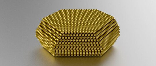
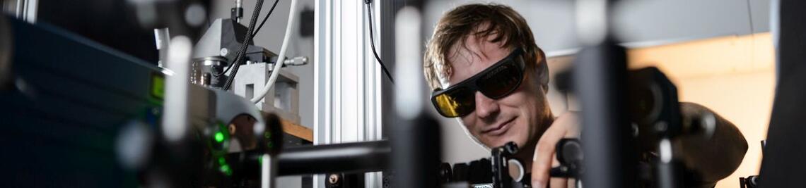
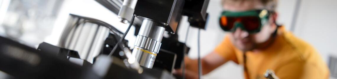
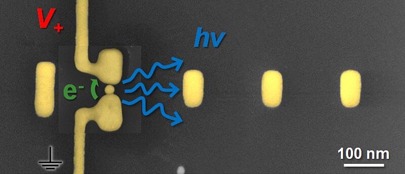
Surface investigation using atomic force microscopy

In order to better understand the surface properties of our nanostructures, we use extremely sharp tips, which are scanned over the sample like a cane.

This systematic scanning allows the topography of nanometer-sized objects to be precisely detected. Furthermore, advanced methods allow us not only to measure the topography, but also the magnetic and electrical properties of nanostructures, to manipulate them or to focus light on an almost atomic scale using special tips.

High-resolution confocal optical microscopy

For the investigation of the optical properties of our nanostructures, we have different, mostly self-made, highly optimized setups available.These allow the structures to be excited by means of laser or white light, so that on the one hand high-resolution imaging is also possible, but also optical spectroscopy can be performed. Important properties such as the optical resonances of the structures can thus be precisely determined or, for example, the photon statistics of quantum emitters can be determined.

Simulations

Finite-Difference Time-Domain (FDTD) simulations

Realistic numerical simulations are an essential tool for us, because in this way the rather expensive fabrication of nanostructures can be planned efficiently. We use two complementary methods.The first is based on the discretization of the space by a fixed grid on which the Maxwell equations are then solved. With the help of a commercial software package, we can predict and optimize spectra, field distributions and radiation characteristics. This method is particularly suitable for complex geometries and problems in the time domain.

Simulationen using the boundary element method (BEM)

The second method is based on discretizing the surface instead of the entire volume. Surface charges and currents are determined, from which the electromagnetic field distribution in the entire volume can be calculated. This method is very fast and suitable for modeling less extensive geometries with curved surfaces. Both methods help us to increase the performance of our nanostructures, to determine the best possible geometries for experiments and to investigate new effects.