
Bachelor & Master positions
We offer Bachelor and Master projects in all of our research areas.
The titles and topics listed below are not necessarily complete. If you are willing to write your thesis with us, please get in touch with the contact person of the field you are interested in.
More information on the topics and research areas of the individual groups can be found on the pages of the group leaders. Simply click on the name link.
Prof. Dr. Sven Höfling
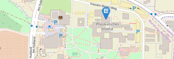
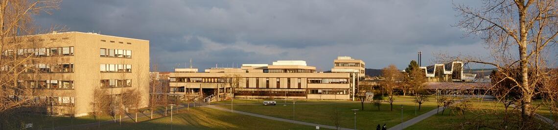
University of Würzburg
Am Hubland
Consultation hours
Tuesday: 14:00 - 16:00
Thursday: 10:30 - 12:00
We are currently offering the following Bachelor theses:
Erforschung der Robustheit von Graphenschichten im Sauerstoffplasma der ALD
We are currently offering the following Master theses:
Elektrische Manipulation von hybriden Zwischenlagenexzitonen in einer monolithischen Kavität
Aufbau eines automatisierten Systems zur maschinellen Suche von Mono- und Multilagen von 2D Materialien
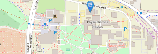
Dr. Simon Betzold
University of Würzburg
Am Hubland
We are currently offering the following Bachelor and Master theses:
Optische Charakterisierung hochreflektierender Spiegel
Experimentelle Realisierung von Quadrupol Higher-Order Topological Insulators
Elektrisch steuerbare Dipolaritonen zur Kontrolle von Wechselwirkung & Lasing
Lichtkontrollierte topologische Randzustände in Polaritongittern
Dr. Fabian Hartmann
University of Würzburg
Am Hubland
We are currently offering the following Master theses:
Interband cascade infrared photodetectors based on InAs/GaSb superlattice absorbers
Topological Insulators based on InAs/GaSb quantum well heterostructures
Dr. Andreas Pfenning
University of Würzburg
Am Hubland
We are currently offering the following Bachelor and Master theses:
Sebastian Krüger
University of Würzburg
Am Hubland