

2021
Image & Results Gallery (2021 archive)
"Construction manual" for quantum materials
June 11, 2021
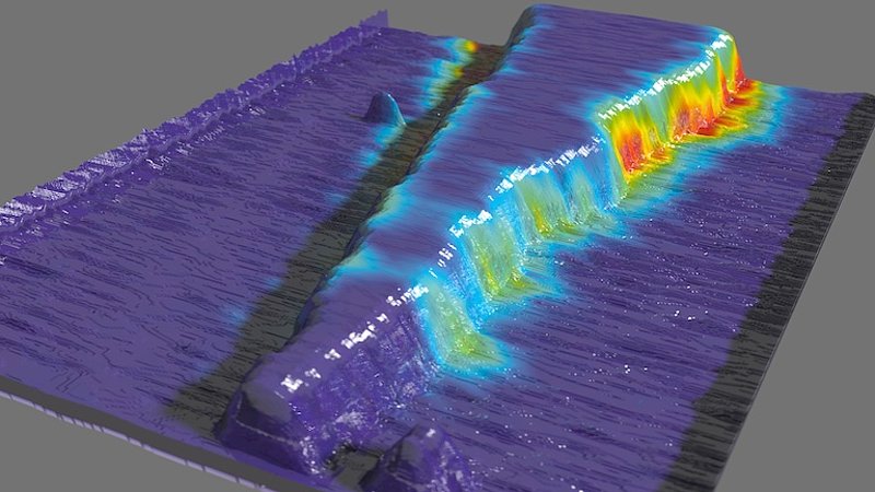
In electronic devices the individual components are connected by wires which route signals from one place to another. Among other factors, the density at which the wires can be packed determines the minimal size of a device. Wires made from topological materials promise to hold some advantages over conventional wires, made, e.g., from copper. For example, topological materials conduct charge almost dissipation-less, thereby reducing losses to a minimum. However, the density at which topological wires can be packed was not known so far. In cooperation with colleagues from the Polish Academy of Sciences we systematically explored how adjacent wires of the topological crystalline insulator lead-tin-selenide interact. The "wires" are created by atomic step edges which naturally exist on the surface between two atomically flat terraces. Some of these edges intersect under an acute angle, thereby forming wedge-like structures where the distance between the edges slowly decreases until it completely vanishes at the apex. The results reveal that the topologically protected states remain essentially unchanged down to a distance of 25 nanometers (nm), a distance which equals a line-up of about 75 atoms. At shorter distances it becomes more and more distorted, as evidenced by a splitting. Eventually, at distances below about 10 nm the topological character of the wires is completely lost, representing the lower limit of how close topological wires can be packed. The results has been published in Phys. Rev. Lett. 126, 236402 (2021).
Anisotropic charge transport caused by single atomic rows
April 7, 2021
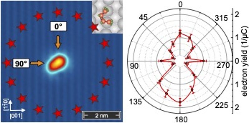
How elementary charges propagate on surfaces or interfaces is of fundamental interest for a myriad of technical applications. Since the building blocks of current electronics products are getting smaller and smaller, the investigation of charge transport on atomic length scales would be highly beneficial. The so-called molecular nanoprobe (MONA) technique, which has recently been developed in our group, uniquely allows for transport studies down to few atom length scales.
In a paper published in Physical Review Letters we report on the first observation of anisotropic hole transport on the (110) surface of face-centered cubic metal Palladium (Pd). Using a single cis-2-butene molecule as a detector, we investigate the transport of charge carriers that are injected by an STM tip a few nanometers away from the molecule. As shown in the sketchat the side, we observe strongly ansiotropic charge transport, with a dip along the the atomic rows of Pd(110) and a peak in the transverse direction. Our measurements provide first evidence that the nanometer-scale charge transport properties of metallic surfaces is significantly influenced by scattering events with single atomic rows.