

Research
At the Chair for Applied Physics (TeP), we combine photonics, light-matter physics and semiconductor nanotechnology to create, control and explore novel physical systems. A recurring theme across many of our activities is the interaction of light with engineered semiconductor and low-dimensional systems, ranging from quantum-light sources and microcavity polaritons to optoelectronic devices and light-induced material phenomena.
A particular strength of TeP is the close connection between materials, fabrication and experiment. Our research covers the complete chain from epitaxial growth and micro- and nanofabrication to advanced optical and electronic characterization. This allows us to develop tailored structures and devices for specific scientific questions and to combine fundamental physics with device-oriented research.
The individual research areas are strongly interconnected and share materials platforms, technology and experimental infrastructure. Prof. Sven Höfling is Head of the Chair and is scientifically involved across several of these areas, while the sections below list the primary contacts for the respective topics. For more detailed information on each research area, follow the link to the respective contact person.
Semiconductor Nanotechnology
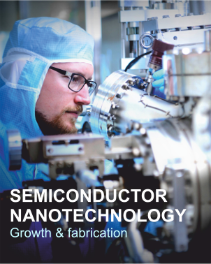
From epitaxial growth to nanofabricated devices
Semiconductor nanotechnology forms one of the central pillars of TeP and provides both an independent research direction and the technological basis for many of our other activities. We develop and fabricate tailored semiconductor heterostructures and nanostructures, with a particular focus on III-V material systems, quantum dots, quantum wells and optical microcavities.
Our capabilities span the complete technological chain from molecular beam epitaxy to micro- and nanofabrication. This includes optical and electron-beam lithography, dry and wet etching, metallization and deposition techniques as well as sputtering, ALD and PECVD. Structural and materials characterization using techniques such as SEM, AFM and SIMS complements the fabrication process.
The aim is not merely to provide fabrication infrastructure, but to develop materials and devices tailored to new physical concepts and experiments. This expertise enables TeP to contribute custom-grown and nanofabricated samples to a wide range of internal and external collaborations, from quantum photonics and polaritonics to nanoelectronics and low-dimensional material systems.
Technology lead: Sebastian Krüger
Scientific lead: Sven Höfling
Semiconductor Quantum Photonics
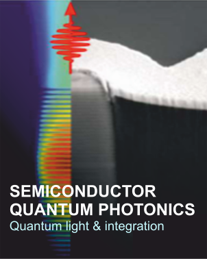
Scalable quantum-light sources and integrated quantum photonics
Semiconductor quantum photonics is a major research area at TeP, combining deterministic quantum-light sources with scalable photonic integration. A central platform is based on semiconductor quantum dots embedded in tailored photonic structures. We investigate single-photon and entangled-photon sources with high efficiency, purity and indistinguishability, covering emission wavelengths from the near-infrared to the telecom C-band around 1550 nm.
A particular focus is the development of sources and photonic interfaces for quantum communication, quantum repeaters and optical quantum computing. Position-controlled quantum dots, microcavities, circular Bragg structures, waveguides and fibre interfaces are explored to improve source performance and enable scalable architectures. Telecom-compatible quantum emitters are especially important for connecting solid-state quantum systems through existing optical-fibre networks.
Beyond individual quantum-light sources, we investigate integrated quantum photonics and active control on chip. Current activities include the integration of III-V semiconductor structures with ferroelectric materials such as barium titanate, enabling fast phase modulation, switching and feed-forward concepts. The long-term goal is to combine high-quality semiconductor quantum emitters with scalable and actively controlled photonic circuits.
Primary contact: Andreas Pfenning
Polaritonics
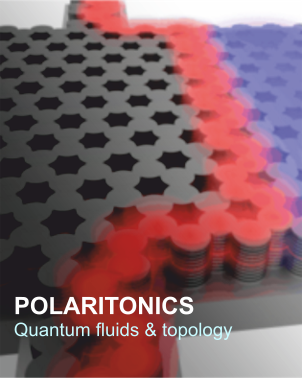
Quantum fluids, topological light-matter systems and hybrid polaritonics
Exciton-polaritons are hybrid light-matter quasiparticles formed through strong coupling between excitons and photons in optical microcavities. Their mixed character combines strong optical accessibility with interactions inherited from the matter component, making polariton systems a versatile platform for studying collective and non-equilibrium phenomena.
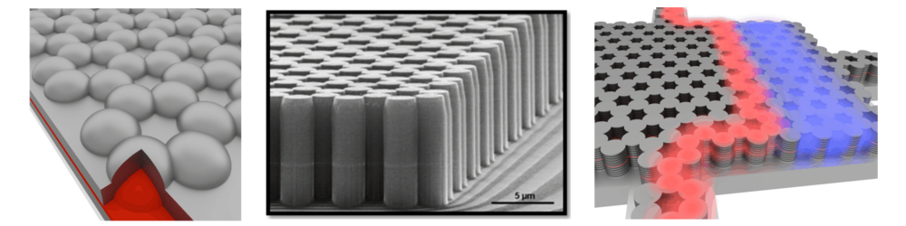
A major focus of our research is the physics of driven-dissipative polariton quantum fluids. We investigate condensation, coherence, interactions and universal non-equilibrium dynamics, including current work on KPZ universality in two-dimensional polariton systems. Beyond conventional condensation physics, we explore topological polariton lattices with edge and corner states, higher-order topology and reconfigurable transport. An emerging direction is light-induced topology, where optical excitation and reservoir engineering are used to locally create, modify or reshape topological states.
A third direction concerns hybrid and electrically controlled polariton systems. This includes dipolaritons, electrically tunable light-matter coupling and hybrid organic-inorganic or low-dimensional platforms. Together, these approaches allow us to investigate how interactions, topology and external control can be combined in engineered light-matter systems.
Primary contact: Simon Betzold
2D Materials
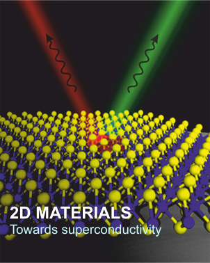
Towards light-induced superconductivity
Two-dimensional materials and van der Waals heterostructures provide a highly versatile platform for controlling excitonic, electronic and optical properties on the nanoscale. At TeP, we investigate transition-metal dichalcogenides and related low-dimensional systems, with particular emphasis on excitons, interlayer excitons and hybrid structures integrated into optical microcavities.
A central goal is to use strong light-matter coupling not only to probe these systems, but to actively modify their electronic properties. Hybrid and interlayer excitons can combine large dipole moments with strong optical coupling and therefore provide a promising route towards electrically and optically tunable polariton states. By coupling such states to two-dimensional electron systems, we aim to explore how collective light-matter excitations can influence electronic correlations and transport.
An important long-term direction is the realization of light-induced material phases, including the prospect of inducing superconducting correlations through optically generated polariton states. More broadly, we investigate how optical, electrical and magnetic control can be combined in 2D heterostructures to create new hybrid states of light and matter.
Primary contact: Sven Höfling
Nanoelectronics
Mid-infrared, topological and neuromorphic devices
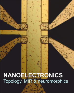
Nanoelectronics at TeP explores functional semiconductor and oxide heterostructures for optoelectronic, topological and adaptive electronic devices. A major focus is mid-infrared optoelectronics, where engineered III-V heterostructures such as type-II superlattices and interband-cascade structures are used to develop emitters, lasers and detectors for sensing, imaging and spectroscopy.
A second research direction concerns topological electronics in InAs/GaSb and related broken-gap heterostructures. These systems provide access to electronically tunable topological states and allow us to investigate the interplay between band engineering, transport and device functionality in semiconductor quantum wells.
More recently, the research area has expanded towards adaptive and neuromorphic electronics. Here, oxide-interface systems such as LaAlO₃/SrTiO₃ are investigated as reconfigurable electronic elements with memristive and memory-like behaviour. Together, these activities combine heterostructure design, nanofabrication and electrical or optical characterization to realize functional devices across a broad range of length scales and applications.
Primary contact: Fabian Hartmann