Würzburg ToCoTronics Colloquium
"Bi2Se3: a layered material with many surprising facets"
| Datum: | 15.01.2026, 16:15 - 18:00 Uhr |
| Kategorie: | Kolloquium |
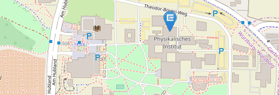
| Ort: | Hubland Süd, Geb. P1 (Physik), HSP P (Röntgen HS) |
| Veranstalter: | SFB 1170 ToCoTronics |
| Vortragende: | Prof. Dr. Daniel Vanmaekelbergh - University of Utrecht/NL |
Bi2Se3 is a layered material consisting of a stack of Se-Bi-Se-Bi-Se quintuple layers (QL) with an overall rhombohedral crystal structure. The quintuple layers are bound by van der Waals forces. Around 2010, it was discovered that three-dimensional Bi2Se3 , i.e., consisting of 7 or more QLs, is a 3D topological insulato protected by a band inversion of about 300 meV. The dispersion of the topological surface state has been characterized by ARPES and scanning tunneling micro-spectroscopy, and modelled by ab-initio and tightbinding models. We have investigated the evolution of the electronic band structure for two-dimensional Bi2Se3, consisting of 1-6 QLs; in these systems the surface states on the top and bottom becomes gapped due to hybridization. I will report on various aspects of 2D Bi2Se3 materialized as nanocrystalline platelets.
(1) We have developed a hot-injection wet-chemical method for Bi2Se3 platelets with a hexagonal shape, lateral dimensions in the 50-200 nm range, and a well-defined thickness in terms of QLs. In addition, we developed a high-temperature vacuum method to prepare macroscopic three-dimensional Bi2Se3 (and related materials).
(2) We have developed a transfer method to transfer the nanocrystals to an ultra-clean substrate in a scanning tunneling microscope. We achieved atomic resolution on the Bi2Se3 platelets on various substrates (gold, macroscopic Bi2Se3). This enabled us to connect the local atomic structure of the Bi2Se3 platelets, including several types of defects, to the local electronic structure. We distinguish defects that do not affect the band structure from defects that result in an extra electronic state not far from the Fermi-level.
(3) For Bi2Se3 platelets of 3-6 QLs in thickness, we found and characterized a state at the edge. According to an 8-band k.p model, and DFT-tight binding simulations this state is a helical edge state of a 2D quantum spin Hall insulator. The band-inversion protecting these states is however weak, and trivial-topological transitions can occur depending on the strain in the material.
(4) We have investigated the optical properties of Bi2Se3 platelets in the near IR and visible. The properties are for a part determined by strong transitions between valence and conduction surface states. We characterized the coupling between the photo-excited electrons and the perpendicular-to-plane Ag phonon modes.
(5) Work in progress: We have stamped Bi2Se3 platelets on macroscopic Bi2Se3 crystals and found that the band structure changes completely. The density of states shows sharp van Hove singularities and hard gaps around the Fermi-level, suggestion moiré physics with strong correlations.
(6) Work in progress: The Bi2Se3 platelets were incorporated in superconducting devices; a ballistic supercurrent was observed at low temperatures passing through the bulk/surface of nanocrystal. When the natural doping was lowered, signatures of supercurrent via the edges was observed.
R E F E R E N C E S
(1) Jara Vliem et al, PhD Thesis Chapter 3, submitted to Small.
(2) Auke Vlasblom, Victor Wesselingh, Ingmar Swart, Daniel Vanmaekelbergh, submitted.
(3) Characterization of the Edge States in Colloidal Bi2Se3 Platelets. J. R. Moeset al., Nano Lett 24, 5110– 5116 (2024).
(4) Role of Surface Bands in the Photogeneration, Cooling, and Recombination of Charge Carriers in Two-Dimensional Bi2Se3. J. F. Vliem et al., ACS Nano 2025, 19, 18, 17261–17272.
(4b) Electron-phonon coupling in 2D Bi2Se3 studied by ultra-fast spectroscopy. Jara Vliem and A. Baserga,
Submitted.